Introduction
I Was Not Into Custom Keyboards
I wasn't collecting switches.
I didn't care about artisan keycaps.
I didn't even have strong opinions about layouts.
My keyboard just broke.
And while looking for a replacement I had one of those dangerous thoughts:
How hard could it be to just build one?
I have a 3D printer.
I know electronics.
I've designed PCBs before.
So instead of adding one to my cart, I opened KiCad.
That's how this started.
From "Replacement" to Architecture
The initial goal was simple: make a clean mechanical keyboard with USB.
But once you're already drawing a matrix and placing diodes, your brain starts adding constraints.
If I'm designing a PCB anyway, why not make the MCU replaceable?
If it's modular, why not experiment with wireless?
If I try wireless, why not do it properly?
That's when it stopped being a keyboard replacement and became a system.
Final Architecture: Two Microcontrollers
I ended up using both microcontrollers.
Not as alternatives.
Together.
flowchart LR
  Matrix["Switch Matrix"]
  RP2040["RP2040 (QMK)"]
  NRF["nRF52840 (BLE)"]
  USB["USB Host"]
  BLE["Bluetooth Host"]

  Matrix --> RP2040
  RP2040 -->|USB HID| USB
  RP2040 -->|UART| NRF
  NRF -->|BLE HID| BLE
The Raspberry Pi Pico (RP2040) runs QMK and handles:
For reference: the QMK project site is qmk.fm and the firmware source lives in the qmk/qmk_firmware GitHub repository.
- Matrix scanning
- Key processing
- USB HID
The nRF52840 handles:
- Bluetooth Low Energy
- Wireless key transport
They communicate over a serial connection.
In practice, the RP2040 remains the "brain" of the keyboard. It scans the matrix and generates key events. Those events are sent over UART to the nRF52, which then registers and transmits them over BLE.
USB mode? The RP2040 talks directly to the host.
Wireless mode? The RP2040 talks to the nRF, and the nRF talks to the host.
This separation kept the BLE complexity isolated from the main firmware logic.
It also made debugging much easier.
Why Not Just Use the nRF Alone?
You can absolutely build a fully BLE keyboard on an nRF52.
But I liked the separation of concerns.
QMK on RP2040 is extremely stable.
BLE stacks can be unpredictable.
Keeping USB and matrix logic independent from BLE logic made the system more robust and easier to reason about.
It also let me experiment without destabilizing the core behavior.
And honestly, architecturally, it just felt cleaner.
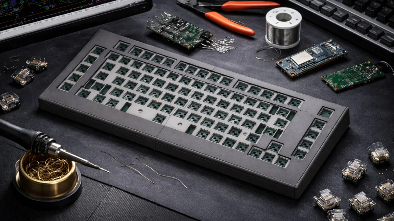
Designing the PCB
The PCB was designed from scratch in KiCad using a classic row-column matrix with per-key diodes.
Nothing exotic. Just disciplined routing.
Rows mostly horizontal.
Columns mostly vertical.
Minimal vias.
Ground pours on both layers.
Decoupling close to the MCUs.
I added a Pro Micro-compatible footprint to keep things flexible.
One important detail was planning the serial link between the RP2040 and the nRF. Proper routing, clean reference ground, and stable power rails matter more when two MCUs are involved.
You're not just routing a keyboard anymore. You're routing an inter-processor link.
Bluetooth Integration Over Serial
The UART bridge between the RP2040 and the nRF52 became the most interesting part.
The RP2040 sends key events over serial. The nRF parses those events and exposes them as BLE HID reports.
This architecture introduced new considerations:
- Latency over UART
- Buffer handling
- Synchronization
- Error recovery
Luckily, the bandwidth for key events is tiny. Even a modest UART configuration is more than enough.
The real complexity wasn't speed. It was state management.
Handling pairing, reconnection and sleep states cleanly required careful firmware coordination.
Power and Battery Design
The BLE side required:
- LiPo battery
- Charging circuit
- Power switching
- Voltage measurement
Once you introduce a battery, you stop thinking like a desktop developer.
Sleep states matter.
Advertising intervals matter.
Idle current matters.
The nRF52 is efficient, but only if configured correctly. Without proper deep sleep, battery life collapses.
Reading battery voltage through an ADC required smoothing and calibration to avoid unrealistic percentage jumps.
This was no longer just a keyboard.
It was a low-power embedded device.
The 3D Printed Case
I designed and printed the enclosure myself.
And this is where theory meets reality.
Because of the size limitations of my printer, I couldn't print the case as a single piece.
So I designed it in two halves, printed them separately, then assembled and glued them afterward.
That changed the problem from "design a case" to "design a case plus an assembly process."
To make sure everything lined up, I used an export of the PCB from KiCad as a reference while modeling the enclosure.
That made it much easier to validate switch positions, mounting points, and cutouts before printing plastic.
3D model of the enclosure, split into two printable halves and aligned against a KiCad PCB export to validate cutouts and mounting points. Click to expand.
USB cutouts need tolerance.
PCB standoff height matters.
Switch plate thickness affects typing feel.
Screws into plastic degrade quickly. Brass inserts don't.
The first version was technically correct and physically slightly wrong.
The second version felt solid.
Iteration wins.
What This Project Actually Taught Me
This was never about becoming a keyboard hobbyist.
It became a small systems engineering exercise:
Two microcontrollers.
Inter-processor communication.
USB HID.
BLE HID.
Battery management.
PCB layout discipline.
Mechanical tolerances.
All because my keyboard broke.
Now every time I type on it, I know exactly which MCU is involved, how the signal travels, and how it eventually becomes a character on screen.
Which makes it very hard to ever buy one again.